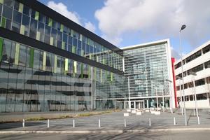
The New Mountbatten Building
The New Mountbatten Building replaces the previous clean room complex, also called the Mountbatten Building, which was totally destroyed in a devastating fire in October 2005.
The new facility has significant advantages: it is interdisciplinary and efficient, significantly shortening device and circuit turn-around times. Although based on Silicon fabrication technology and largely using Silicon substrates, the new clean room is not aligned with a core Silicon process, such as Bipolar technology or CMOS technology. Instead, the deep-submicron capability afforded by equipment such as the JEOL direct-write electron beam lithography system means that we will concentrate primarily on structuring, modifying and characterizing materials at the nanoscale.
These materials will include Silicon, but will also enable polymers and more exotic materials such as Zinc Oxide, high-refractive index metallic oxides, and lithium niobate to be nanostructured. By studying the practical solutions to structural and optical problems provided by Nature (biomimetics), we will create a new generation of unique nanodevices, which will satisfy the ever-increasing needs of society.
The building contains:
- 600m2 novel electronic devices clean room
- 110m2 bio MEMS clean room
- 110m2 thick film MEMS clean room
We have the capability to fabricate
- glass-based devices
- thin film devices
- solar cells
- micro-fluidic devices
- silicon-based devices
- photonic devices
Essential equipment for the building includes:
- Electron beam lithography with a 5nm resolution
- FEGSEM
- Epitaxy for SiGeC growth, Ge quantum dot growth, in-situ doped polycrystalline and amorphous SiGeC
- Atomic layer deposition
- Bosch process deep silicon etcher (in new lab)
- Aligner/bonder (in new lab)
- CVD carbon nanotube growth (in physics already)
- E-beam evaporator
- Sputterer for metals and insulators
- Ion beam milling/deposition (in new lab)
- PECVD Nanofab for Si and Ge nanowire growth
- PECVD Oxide and nitride deposition
- PECVD high lifetime polysilicon deposition for solar cells
- Rapid thermal annealer
- Furnaces
- General optical lithography and dry-etch capability
- Wet chemistry room
- AFM
- General metrology equipment for layer thickness measurement
- DC on-wafer device characterisation
- RF device characterisation